
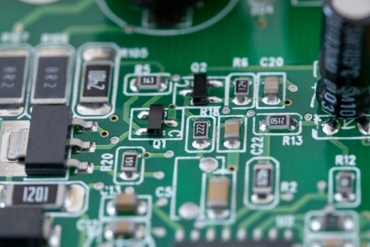
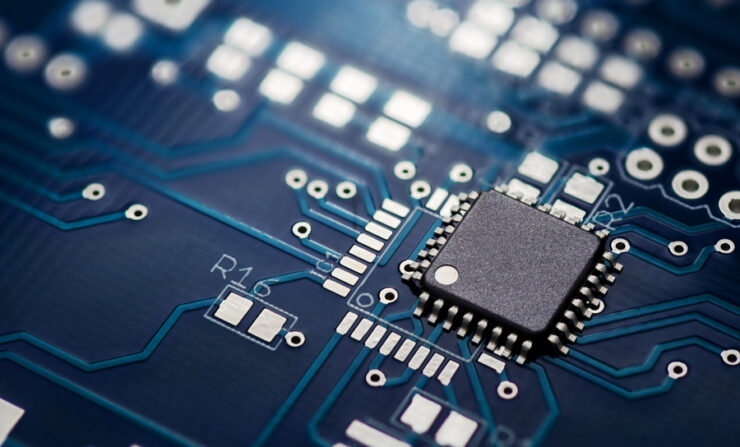
In every electric circuit, PCB is a base to attach components and create an effective electrical connection. Even if you make a small error, it can fail your circuit. All your hard work will go to waste and should be avoided. You need to be careful while placing any component in the PCB.
But many people make common mistakes and need to receive the desired output. Make sure you know about such flaws and do your work with care. In this write-up, you will learn about the regular mistakes people make while placing components on PCB.
You must avoid them to get the desired output. You need to select the right devices to attach to the PCB so that the electrical circuit completes and your connection becomes smooth. It is necessary to understand the basic functioning of the components you are attaching to the board and determine the perfect way to place them.
1. Choosing Incorrect Trace Geometry
It is crucial to understand the PCB tracing geometry, where you can build a good connection between all types of components. The thickness and width should be of appropriate size. You cannot consider standard width for small types of circuits. You can get help regarding the PCB assembly by uetpcb.com.
If you do so, a high current will reach the devices, and it can destroy the circuit. The board will heat up, and you will not get the desired outcomes. It is crucial to determine the correct thickness as well as the width of the PCB to attach available components to it. You must track power and current units to confirm whether the device will work. You must understand the trace and choose the one that goes well with your circuit.
2. Incorrect Layout
A massive demand is for small PCBs for creating compact electrical circuit designs. Forcefully, you will install devices available with small footprints together at a small distance. It is the biggest mistake you can make, and you must avoid it. This incorrect layout can risk your connection and produce non-compliance regarding issues.
You cannot connect any device with a higher number of pins on the PCB. Choosing the layout wisely matches well with your circuit is necessary. There is no need to follow the common trend that everyone is following. You must keep the correct concepts and follow them to get perfect results.
3. Incorrect Position of Capacitors
You must install a decoupling capacitor to provide stable power without oscillations to all the attached components. It is quite essential to connect them in parallel with the given power supply, and it must be quite close to the attached device pins for providing power.
The line for providing power to the devices must be clear and well-routed. Before you attach the capacitor, ensure it receives stable voltage. You cannot add devices to the board randomly, and it is necessary to check all the units correctly.
You need to consider all the factors so that the capacitor works as you need. All the components will not get sufficient power, and it can also break the circuit. It is essential to stabilize the voltage connection to get stable power throughout the circuit from the capacitor.
4. Error in Landing Pattern
Many use terms, i.e., landing pattern, as a footprint or vice versa. But you must understand that these terms are slightly different. The landing pattern means the pad size must be larger than the footprint for every component. If you make a little spacing mistake, the circuit will not work.
Before placing it on the board, you must go through the landing pattern for every component. This mistake is quite uncommon, and many people do not even realize it. If you keep the distance between the pins less than one mm, the devices will not be properly aligned.
To avoid this mistake, you must go through all the standard designs with dimensions. Many people do not even know about it because they consider the landing pattern the footprint. They experiment with the board without knowing a slight difference.
5. Incorrect Layout of Antenna
An antenna is attached to the PCB for proper wireless communication. It is crucial to place this device carefully considering the layout mistake. If you want to enhance the transfer of power, it is crucial to do the impedance adaptation between the receiver and the antenna.
It is crucial for the transmission line that connects to the antenna as well as the transceiver with an impedance of at least 50 ohms. With the help of a tuner filter, you can modify the circuit impedance for getting the correct output. Before you place the antenna, make sure that you consider the impedance on the board.
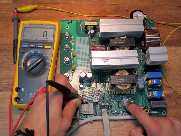
6. Not Checking the Circuit
When you connect components to the PCB board, it is necessary to check all the connections by revising the circuit. It needs to be done before providing a power supply to the devices. If everything you attached seems alright, then you can go ahead to see the output.
If you find any issue, you must immediately correct the placement of the devices. Many people need to check what they have connected to the board, and they expect their circuit should work smoothly. It is a must step that should not be avoided.
The Bottom Line
PCB boards are available in different sizes and layouts. You can attach components to it and make a circuit. But you can only randomly place things and expect things to go well. It is crucial to check all the electrical units and whether the devices are placed correctly. For correct placement, you must determine more about different landing patterns, padding spaces, etc.
Chances are there to make regular mistakes mentioned above, and you must avoid them in any way. You must check out all the errors you might be making, leading to incorrect results after so much hard work. Take care of these mistakes and improve component placement on the board.