
Printed circuit boards are everywhere around us, and manufacturing and assembling them can be an extremely long and complex process. If you have been interested in the manufacturing of these boards, you have come to the right place. In this article, we are going to give you several tips for understanding the PCBA manufacturing process and we will help you learn more about it.
1. It starts by creating the design
The whole process starts with creating the design. There has to be a plan and blueprint for what the PCB is going to be used for and which requirements would it needs to abide by. This is done using specialized design software, and the designers can easily create and modify the plan. Once the design is created, it can be used for just one exact batch of boards and it can also be utilized in the future as well.
During the designing process, and creating the plan, experts are included and things are tested and inspected even before the assembly starts. This is crucial so that errors can be minimized for future steps.
The PCB manufacturing as well as the creation of the design may differ depending on the manufacturer, and you can learn more about the design and layout process by visiting https://pcbasic.com/.
2. The design has to be approved
Once the design is created it has to be reviewed and checked. Engineers will ensure that there are no missing parts in the plan and that all the components are located where they should be. In case the engineers have any questions when it comes to the plan, this is the step where they ask the questions before proceeding with the manufacturing.
In case something is missing, or if the design has any flaws, then it is returned to the designers with notes from the engineers on how to improve the look and what they need to change or add.
3. The design is printed along with all the layers
After the design is approved the next step is printing out the board as well as all the layers and components. All of this is done using different devices, and the whole process is relatively quick and easy. Once all the information is given to the software, the only thing needed is to wait until every component is printed. There are two main colors that are represented in the circuit board and they include black and clear ink. During this step, the copper for the interior layers is printed as well and it is later on washed with an alkaline solution to remove any unwanted particles. Once the board is washed, it is left to completely dry before the next steps.
4. Everything has to be aligned before soldering
Once all the components are printed and if everything goes according to plan, the components have to be aligned on the board before the soldering can begin. During this step, a visual inspection is done so that the engineers can see if there is an error with any of the components or the board itself.
Once that is inspected, the next step is putting the soldering paste in the cavities of the board where the components will be later on set. The soldering paste is not put on the whole board but instead, it is pushed only in the holes or the cavities. In some cases, degradable glue is used to keep the components in place before everything is soldered together.
5. There are exact assembly steps that have to be followed
There are exact assembly steps that have to be followed and they cannot be skipped without negatively impacting the board full stop. Every part has to be inspected before the assembly starts and the damaged ones have to be discarded. The more complex the board is, the more steps for assembly it will require and the minimal number of steps that have to be included are between four and six.
6. The process may involve up to 20 steps
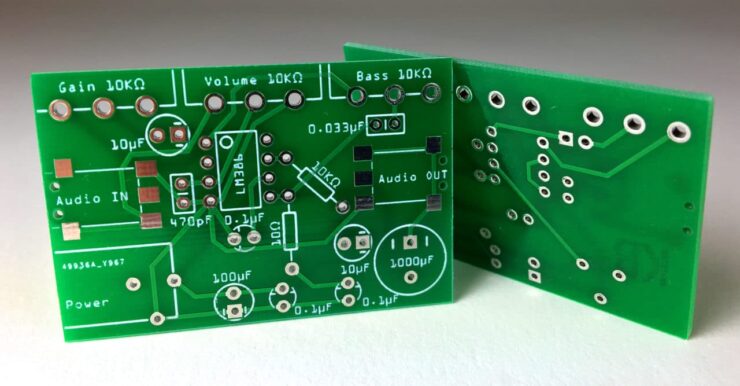
Keep in mind that this process can be different for different types of PCBs. There are three main types of printed circuit boards, and they include single, double-layered, and multilayered and there can be major differences in the structure of the boards.
Because of this, some manufacturing processes are going to require up to two dozen steps and they can differ depending on the type of board that needs to be produced and assembled, as well as the manufacturer themselves. The more complex the board is, the more steps of assembly it will require. Note that in case the steps are skipped or missed, this can negatively impact the performance of the PCB.
7. Inspection and feedback are required
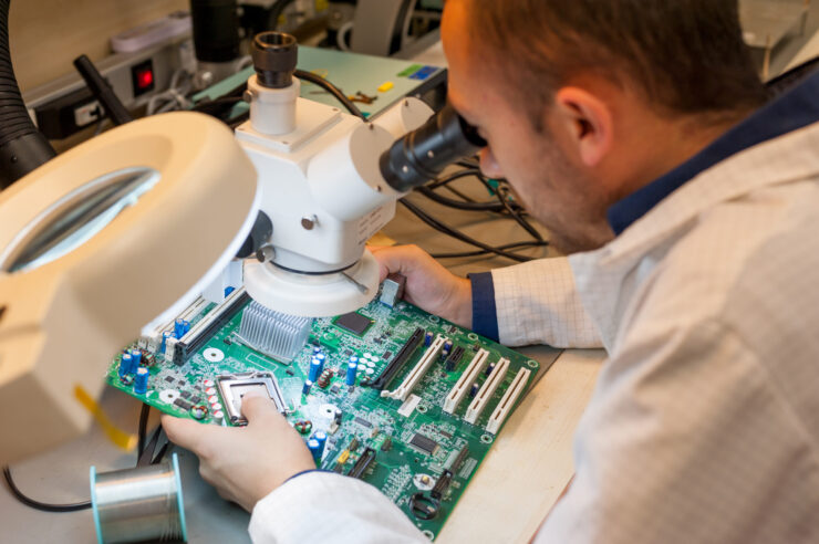
The last step of the PCBA manufacturing process is inspection and feedback. During the assembly process, as we previously mentioned, the components will be checked and test it. During the process, most of the testing involves visual inspections. These inspections can show if there is physical damage to the board or if something is missing, however, they cannot show if there are any in-circuit problems.
Because of this, before all the components leave the factory, they have to be thoroughly inspected and tested. If there are components that are not properly working, or if they have any type of defect, the testers and the operators are required to submit feedback and explain what was not properly working and why. Depending on the mistakes and errors some of the steps may be revised for the next batch of PCBs.
As you can see this manufacturing process may be extremely complex, and not everyone can understand everything up to the smallest detail. If you want to know more about the whole process and what is done within each step, you can always reach out to a manufacturer and get your questions answered. In case you want to collaborate with a manufacturer, it is always advised to reach out to those who have the needed skills, experience, and expertise.